
Introduction
The aim of this project was to design a 16 point Discrete Time Fourier Transform (DFT) on FPGA (Xilinx SPARTAN XC3s500E on Starter Kit). The specific application was to get the signal in floating point format in a block of 16 point (each point is therefor 32 bit) and calculate the Fourier Transform to obtain the most significant energy domain(which frequency has the most part of the signal’s energy). Meanwhile the goal is to have this operation Fast and Area-Efficient to use the minimum possible area on the FPGA. So we used FFT to get the speed and we designed our own Finite State Machine (FSM) to reach the both goals.
Getting Speed
DFT is defined as:

So to calculate the N point Fourier transform on N point signal we need to calculate (when storing the value of exponential terms as look-up-table and not calculating them):
– N complex sums
– N complex multiplications
for each X[i]. So to calculate all N value of DFT we need to do this N times. Since the addition is far less complicated compare to multiplication, we can ignore sums and as a result this simple algorithm needs O(N^2) multiplications and so is not fast enough. To get the desired speed we will use the following algorithm.
To get the fast implementation we used Cooley–Tukey FFT algorithm and Butterfly structure as shown below.

figure1. Butterfly structure
By using this structure we need to calculate N complex multiplications and N complex additions at each stage and since we should do this log(N) times then we have the algorithm with the complexity of ~O(N log(N)) which is currently the state-of-art.
Implementation
Having in mind that we needed the area-efficient design we design the FSM as follows.
To have the least area we used only 2 RAMs back & forth by going forward in each stage of butterfly structure. We need to compute the complex multiplication at “Odd” stages and complex addition in “Even” stages, naming the first stage 0. So we had to design a module called “complexMultAdd” (CMA) to perform complex multiplication and addition using the least area possible by “Resource Sharing Technique” on 32 bit IEEE 754 standard floating point numbers by selecting the appropriate control signals at each time.
FSM
Our total FSM is a three level FSM. The most outer layer one is called “Stage” and is the state of where we are in the terms of stages on butterfly structure. So it is important if it is odd or even number so then we perform different operation. The next layer is called “Phases” which is actually inside each stage and performs the appropriate control signals that we need for reading form specific index of memory, giving it to the CMA and setting the correspondence control signal of this module, wait until the “ready” signal of CMA is 1 (it shows the calculation is finished) and at last storing the results in the correct location in the other memory. Take into account that in the butterfly structure at each stage the operand of calculation is different and should be calculated based on the which stage we are in. The last layer FSM is simply a chain( a.k.a counter) which sweeps each memory entry from up to down. Note that at some point we need to flip the sign bit as is shown in the structure. We have optimized the functions that determines the sign bit, index of array and mode of operation of CMA as a function of stage and phase and counter.
For calculating the absolute value of each DFT value result, we just need to do one more stage but with giving the CMA same memory entry but with flipped sign bit of imaginary part of one of the inputs because in complex manipulation we have:
C = a + i b
|C|^2 = (a + i b ) * (a – i b)
This approach can easily be implemented in our design with few changes in control signals of CMA. And at the end we sweep among all entries and will find the maximum value. Also we will show the frequency on the seven segments on the board.
Simulation with ISim
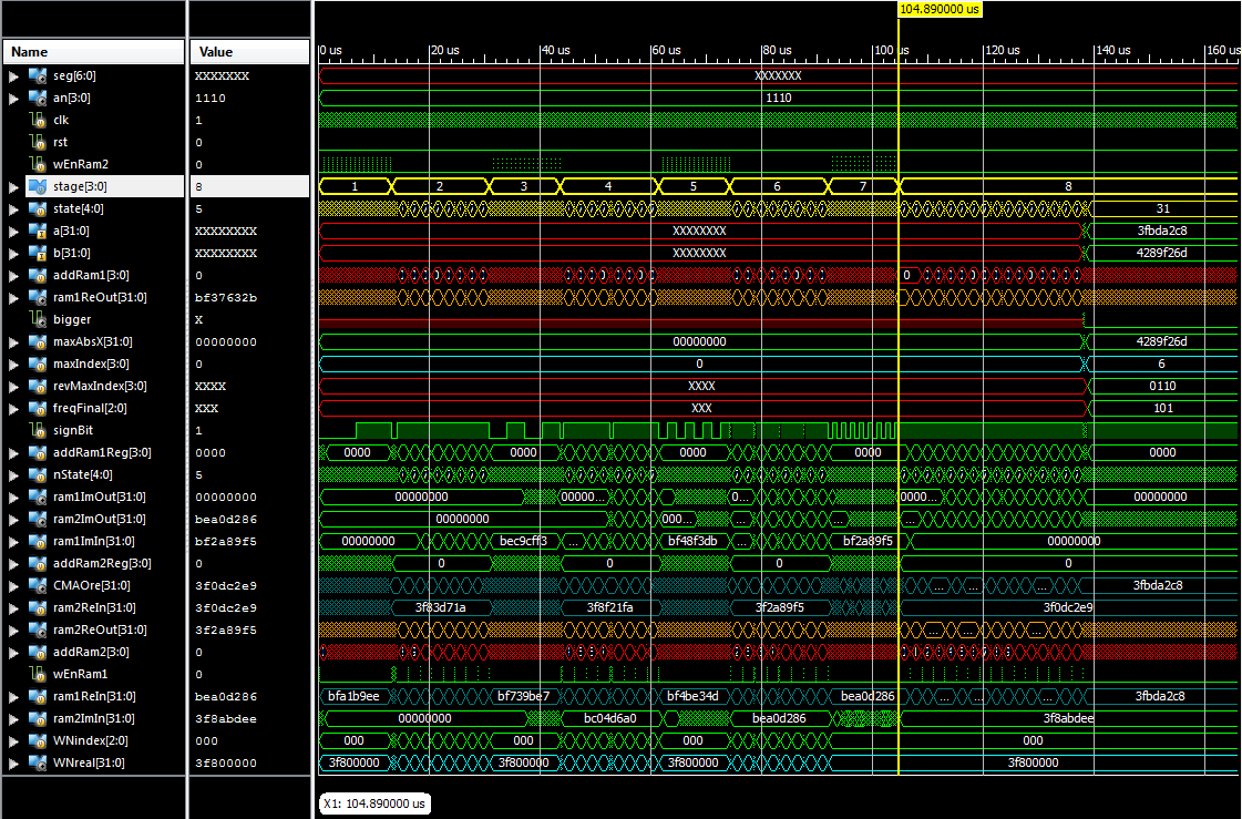 figure2. All stages in one screen
As we discussed at each stage we have different states (a.k.a phases).
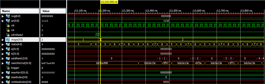 figure3. Different states in each stage
Results
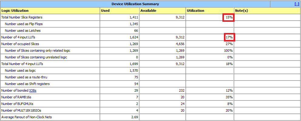 figure4. Results
The figure 4 is results of this implementation and as can be seen has used only 15% of total slice registers and 17% of 4-input LUTs.
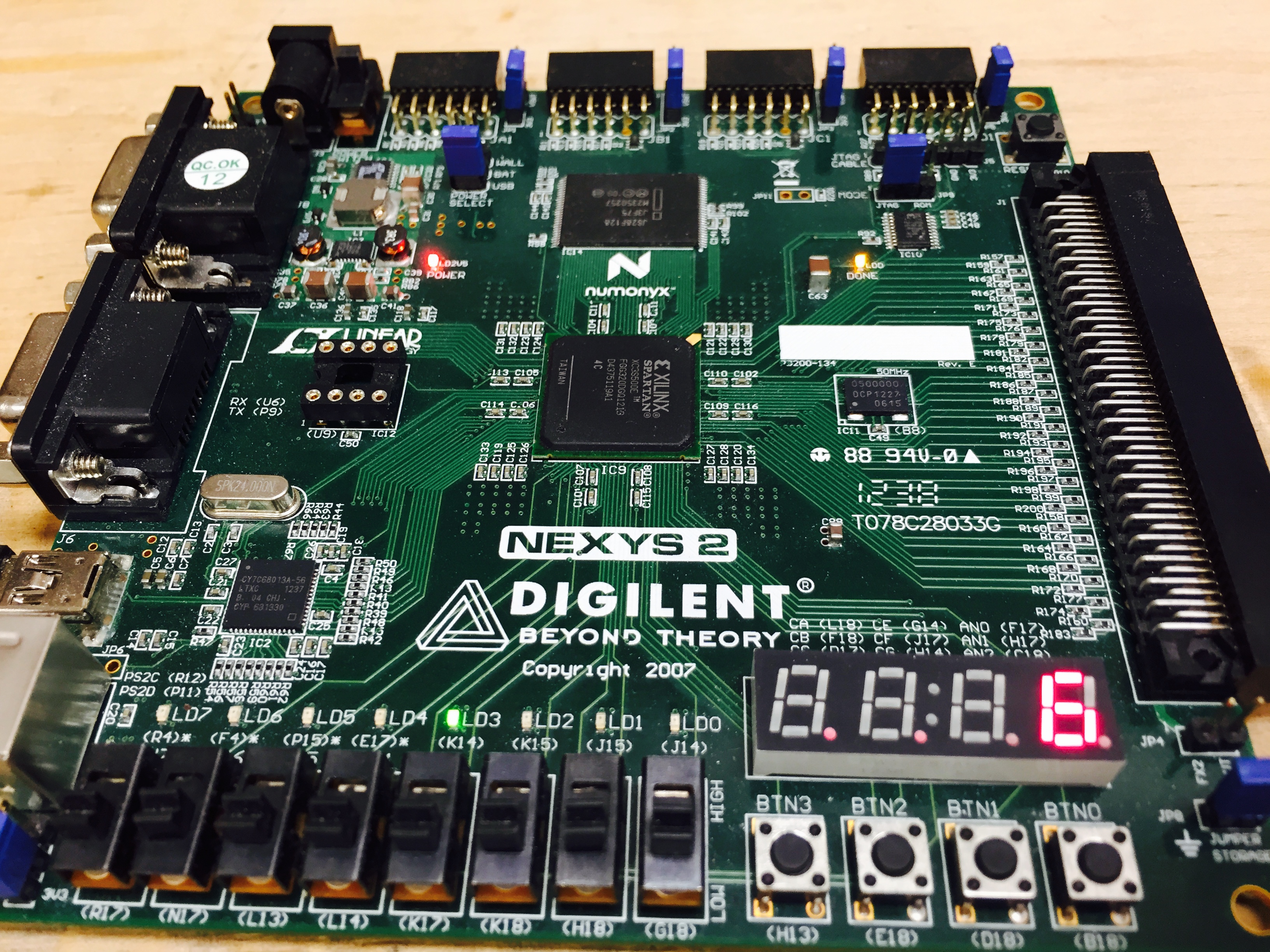 figure5. final implementation and frequency result on FPGA
References
– Wikipedia
Source Codes
Xilinx ISE Project
MATLAB
This project was done by a group of three persons including me, Seyed Mohammad Kazempour(Designing CMA) and Hamed Rahmani(MATLAB code) in December 2014.